





Description
Key Technical Specifications
| Parameter | Value / Specification |
| Part Number | XVC768AE102 / 3BHB007211R0102 |
| System Framework | AC 800PEC Platform (Power Electronics Controller) |
| Control Interface | Dynamic real-time FPGA matrix paired with high-performance RISC processor |
| Communication Array | High-density onboard optical fiber channels for localized peripheral links |
| Input Nominal Supply | 24 V DC (Backplane derived via stable rack bus) |
| Logic Execution Rate | Sub-microsecond processing cycles for inner current/voltage vector loops |
| Environmental Shielding | Industrial-grade conformal coating for moisture and airborne particle defense |
| Cooling Profile | Forced-air via system chassis enclosure fan assemblies |
| Operating Temperature | 0 to +60 °C |
| Weight | 1.52 kg |
Product Introduction
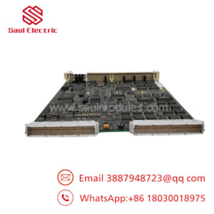
The ABB XVC768AE102 3BHB007211R0102 is a high-performance processing and fieldbus interface master board built within the AC 800PEC controller architecture. This card operates at the critical control level of multi-megawatt power electronics systems, executing the rapid mathematical transformations and closed-loop vector algorithms necessary to control high-capacity IGBT and thyristor semiconductor bridges. By integrating a dedicated real-time FPGA matrix alongside an advanced processor core, it updates firing commands within sub-microsecond timelines.
This module is a core component in specialized, high-power automation environments, such as static synchronous compensators (STATCOM), gas turbine starter systems (MEGATROL), and large-scale industrial variable frequency drives. The XVC768AE102 depends on an array of front-panel fiber-optic transceivers to transmit gating parameters directly to distributed gate drive units. This optical configuration separates the digital processing electronics from the high-voltage interior of the power converter enclosure, providing total immunity against high-frequency electromagnetic interference (EMI) and electrical transients.
Installation & Configuration Guide
Stage 1: Pre-Installation Preparation (Estimated Time: 15 minutes)
- ⚠️ Safety First: Isolate the control rack and the associated converter power bridge from all high-voltage grid lines and auxiliary 24 V DC power sources. High-power converter enclosures store lethal levels of residual electrical energy inside their DC-link capacitor networks. Lock out and tag out (LOTO) all supplies. Wait a minimum of 15 minutes for internal stored energy to naturally discharge down to safe voltage parameters (<50 V). Confirm complete isolation with a calibrated high-voltage multimeter before un-slotting components.
- Tools Required: Grounded anti-static (ESD) wrist strap, Pozidriv PZ2 screwdriver, industrial-grade fiber-optic cleaning swabs and fluid, component markers, smartphone.
- Data Backup: The XVC768AE102 hosts custom compiled control programs and site-specific operational application settings within its non-volatile memory. Ensure you have an updated, valid software backup copy of the target control project (compiled via MATLAB/Simulink or ABB Control Builder M) available on the engineering station before proceeding.
Stage 2: Removing the Old Module (Estimated Time: 10 minutes)
- Secure your ESD wrist strap and connect its grounding clamp to a bare, unpainted surface of the metallic control cabinet frame structure.
- Label each incoming fiber-optic cable and copper communication line connected to the card faceplate. Fiber pairs must be reinserted into their exact original channel mapping locations during reassembly or timing sequences will fail.
- Carefully unlatch and extract the optical fiber plugs. Immediately place clean protective dust caps over both the detached cable tips and the board’s open optical transceiver ports to prevent airborne dust accumulation.
- Back off the top and bottom captive retaining screws that anchor the XVC768AE102 faceplate into the rack chassis frame.
- Draw the card straight forward along its slot tracking channels. Keep the board flat and stable to avoid scratching the surface trace components against adjacent cards. Place the pulled card inside a protective anti-static bag.
Stage 3: Installing the New Module (Estimated Time: 15 minutes)
- Extract the new XVC768AE102 board from its factory static-shielding package while maintaining a secure personal grounding link.
- Configuration Clone (Crucial): Check the physical surfaces of the new PCB for manual micro-dip switch banks or rotary address selectors. You must set these hardware switches to match the exact pattern of the old board. These hardware toggles dictate the module’s target network address, sub-bus hardware parameters, and initial system boot logic.
- Slide the card into the slot guide tracking arrays, ensuring the rear card edge aligns smoothly with the backplane connectors. Push firmly until the board links home, then secure the top and bottom captive screws.
- Clean the optical fiber tips using a specialized lint-free fiber tool. Remove the temporary dust covers and plug each fiber cable back into its corresponding port, making sure they click into place.
📋 Self-Checklist:
- [ ] All onboard hardware dip switches match the legacy board configuration exactly.
- [ ] Fiber-optic connectors are cleaned, verified unbent, and fully seated.
- [ ] Retaining faceplate screws are tightened completely to establish a solid chassis grounding bond.
Stage 4: Power-On & Testing (Estimated Time: 20 minutes)
- Energize the 24 V DC auxiliary control power rail first, keeping the primary medium-voltage power bridge completely isolated.
- Monitor the faceplate status LEDs immediately upon power application. A normal startup sequence transitions past internal self-tests to a steady green RUN status indicator. A solid or blinking red ERR/FAULT light suggests an address configuration mistake or a boot self-test failure.
- Connect your engineering laptop to the configuration port or access the node over the supervisor network to verify the module’s presence in the controller hardware tree.
- Download the site-specific application file and parameter tables to the newly seated module.
- Once code loading is complete and communication lines show clean status, safely restore main power and perform a dry run of the converter to verify stable gate feedback telemetry.
- ⚠️ Troubleshooting Note: If the system engineering console flags an immediate “Optical Link Failure” or a communication timeout after booting, verify that the fiber cables are not crossed (TX line mistakenly crossed into an RX port) and confirm that the cable tips were properly cleaned before insertion.
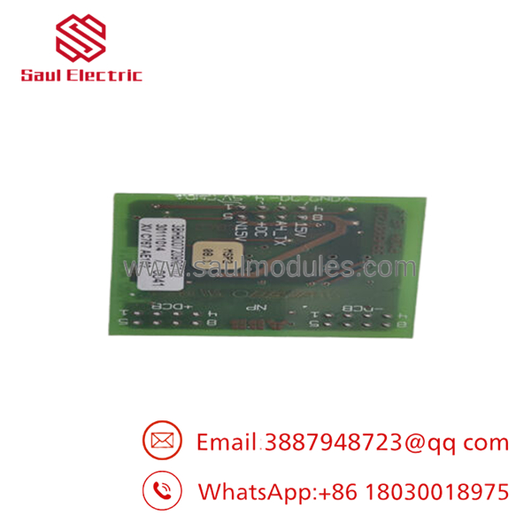
- 3BHB007211R0102
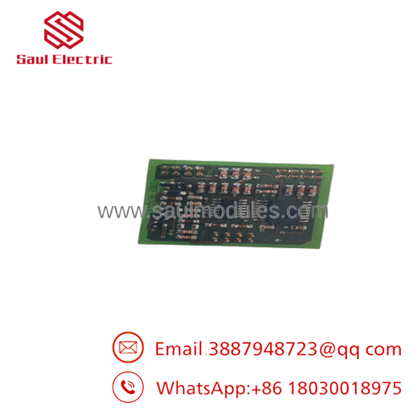
- 3BHB007211R0102
Frequently Asked Questions (FAQ)
Can the card be hot-swapped while the power electronics system is running?
Because this board regulates microsecond-level switching signals for high-capacity semiconductor gates, disconnecting it mid-operation will instantly break the active regulation loop. This results in an immediate high-energy system trip and can cause severe, explosive hardware failure inside the thyristor or IGBT banks due to out-of-phase commutation spikes. Always take the system completely offline before performing a swap.
What is the distinction between model identifier and code 3BHB007211R0102?
is the functional model classification code used by engineering teams to identify the hardware family, circuit revision architecture, and option variant. The string 3BHB007211R0102 represents the exact factory part number assigned by ABB for logistics, order matching, and manufacturing trackability. Both identifiers must match to ensure a drop-in replacement that aligns with your drive software configuration.
What function does the integrated FPGA core perform on this board?
Standard industrial processors are excellent at handling general sequential logic (like reading temperature sensors or processing alarms), but they are too slow to calculate the microsecond-level changes required for multi-megawatt power electronics switching. The real-time Field Programmable Gate Array (FPGA) on the handles these critical loops in pure hardware circuits, allowing the system to adjust pulse-width modulation (PWM) signals instantly to counter grid imbalances or load jumps.
Does this replacement board include our specific plant control logic or parameters pre-loaded from stock?
No. Replacement units supplied from factory stock or surplus warehouses are delivered with standard system boot-level firmware only; they do not contain your specific plant configuration layouts, motor curves, or synchronization variables. You must connect your engineering tool (such as S+ Engineering, Control Builder, or MATLAB) and perform a complete program configuration download to the unit before it can actively manage field operations.
Why is the conformal coating critical for the lifecycle of the ?
Because this module is deployed in aggressive environments like marine engine rooms, heavy chemical facilities, and metal processing mills, the air often contains high humidity, metallic dust, or corrosive trace gases. The factory-applied conformal coating provides a protective layer across the circuit traces, preventing tracking faults, electrical shorts, and moisture-driven corrosion to ensure reliable system operation over many years.

 Start Chat


